


RAPID PROTOTYPING
UltraFast® Rapid Prototyping
Rather than waiting weeks for your critical prototypes, UltraSource is guaranteeing them in a matter of days, cutting your time to market, improving the integrity of your designs, and ensuring long-term repeatability as you hone your designs to perfection.
UltraFast® Rapid Prototyping Program Details
This is the new economy. Time is the biggest enemy of designers creating the next generation of breakthrough products. Since 2010, the UltraFAST® program has enabled our customers to bring their products to market faster than ever before at an amazing 99.9% on-time delivery!
To meet the challenge of these aggressive deliveries, we’ve dedicated an entire team to the task of creating a streamlined manufacturing approach. With our expertise, you’ll be testing your prototypes faster than ever before. In addition, UltraFAST® is designed to offer a selective range of standard single-sided and double-sided designs compatible with a broad range of traditional thin film circuit requirements. The substrate choices, metalization systems, and integration options have also been selected to allow you to further increase device function and performance while reducing prototyping costs.
The Approach
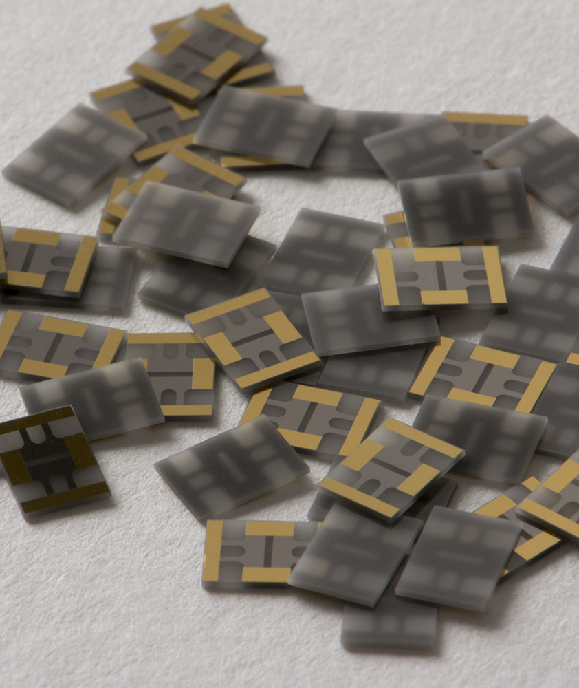
In evaluating the varying requirements of our customers, UltraSource has identified four circuit types for rapid prototyping:
- 4 Days: 1-Sided Conductor
- 5 Days: 2-Sided Conductor
- 6 Days: 1-Sided Conductor with Resistors
- 7 Days: 2-Sided Conductor with Resistors

The Possiblities
At UltraSource, we specialize in working with our customers in order to provide innovative products and services. We realize that the standard options available through the UltraFAST® program may not provide the requirements for every customer.
If you need a metal, material, or features that are not listed in the UltraFAST® standard options, please contact your local sales representative or our corporate sales office to discuss how we can customize a rapid prototype program for you.
UltraFAST® RAPID PROTOTYPING SPECIFICATIONS
Standard Order & Design Criteria
| To Quote & Order | Enlist in the Standard or Custom UltraFAST® program by contacting your USI Sales Representative |
|---|---|
| Standard Pricing | Per the UltraFAST® Price List |
| NRE Charges | FREE (included in pricing) |
| Shipping | FREE (included in pricing) |
| Design Rules | Per the Furnished UltraFAST® Design Templates |
Standard Material & Metalization Criteria
| Available Substrate Materials | Polished 99.6% Alumina | Polished Aluminum Nitride |
|---|---|---|
| Substrate Thicknesses | 5, 10, 15, and 25 mil thicknesses | 5, 10, 15, and 25 mil thicknesses |
| Available Front Side Metalization Schemes |
Option 1: 50 Ω/sq. TaN/500 Å WTi/4 μm Au
Option 2: 500 Å WTi/4 μm Au |
Option 1: 50 Ω/sq. TaN/500 Å WTi/4 μm Au (not available on AlN with PTH) Option 2: 500 Å WTi/4 μm Au |
| Available Back Side Metalization Scheme |
500 Å WTi/4 μm Au | 500 Å WTi/4 μm Au |
| Minimum Line or Spacing | .001″ (25 μm) | .001″ (25 μm) |
| Pattern & Etch Tolerance | +/- .0002” (+/- 5 μm) | +/- .0002” (+/- 5 ) |
Standard Product Type Criteria
| Product Type | Conductor Layer on 1 Side Only |
Conductor Layer on 2 Sides (front & back) |
Conductor & Resistor Layer on 1 Side Only |
Conductor Layer on 2 Sides (front & back) plus Resistor Layer |
|---|---|---|---|---|
| Build Time | 4 working days | 5 working days | 6 working days | 7 working days |
| Quantities | Yield from 2 substrates* | Yield from 2 substrates* | Yield from 2 substrates* | Yield from 2 substrates* |
| Back Side Metal | None | Yes | None | Yes |
* Limited to 50 individual pieces per part number
Standard Options Criteria
| Options | Comments | Build Time |
|---|---|---|
| Multiple P/N Design (Pizza Masking) | Allows for prototyping of a maximum of 4 part numbers on the same photo & substrate | + 2 or 4 working days added to standard build times depending on complexity |
| CopperVia™ | Provides assembly, thermal, or transmission benefits from solid copper filled vias, includes custom sputtering (not available in 5 mil ceramic thickness) |
+ 15 working days added to standard build times |
| Plated Thru Holes (PTH) | Offers grounding of selected circuit features, includes custom sputtering | + 5 working days added to standard build times |
| Post Laser Features | Allows chamfers, pockets, or radii to be added to circuit features | + 2 working days added to standard build times |
| Laser Trimming | Offers the ability to trim individual resistors to +/- 1% tolerances | + 2 working days added to standard build times |
| CAD Conversion | Convert supplied CAD drawing(s) into format suitable for UltraFAST® | + 1 or 2 working days added to standard build times depending on complexity |
NOTE: Please contact USI for current pricing, delivery, and option offerings.