


Search the UltraSource Website
UltraSource – Your Thin Film Source
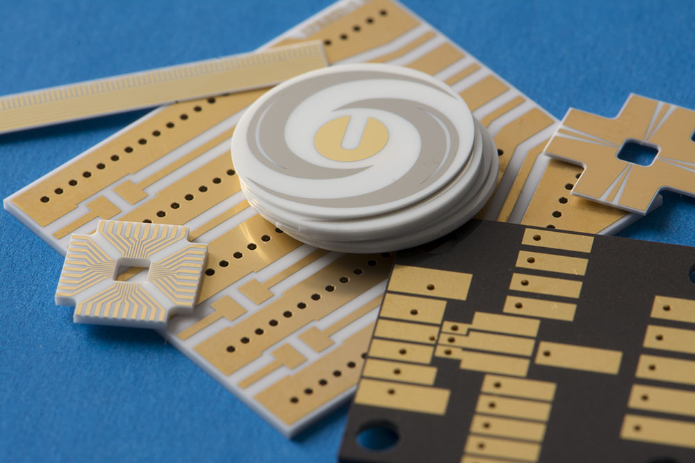
UltraSource provides build-to-print thin film manufacturing services for a diverse set of high technology companies.
UltraSource, a Vishay Intertechnology company, is one of the most advanced thin film circuit and thin film interconnect manufacturers in the world.
Our 25,000 square foot facility in southern New Hampshire houses a complete array of cleanrooms and equipment specially tailored for manufacturing reliable, high-quality thin film products. UltraSource was founded in 1991 and acquired by Vishay in 2018.
UltraSource is an industry leader in high-performance thin film circuits and thin film interconnects. UltraSource products are used in many applications demanding zero failures and zero downtime. UltraSource is AS9100 certified, attracting and retaining customers in aerospace, defense, satellite, and medical industries where quality and high reliability is an absolute must.
UltraSource has developed a comprehensive scheduling and planning software system that enables us to manage supply and demand. Complex manufacturing routings are programmed with set up and run times, and the software system schedules the work centers in the factory.
UltraSource provides customers with the ability to create a wide variety of high-performance, extremely reliable circuits for critical applications, such as defense and space.
What is Thin Film?
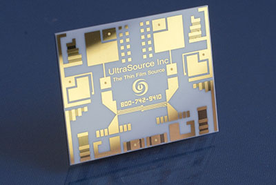
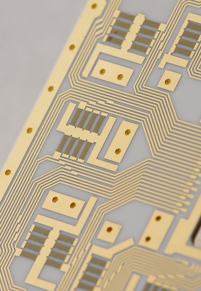
Thin film is the term used to describe a circuit technology used to fabricate devices for a variety of electronic and optical applications.
The thin film circuit patterns are defined using photolithography (photoresists and photomasks).
Thin film circuits are machined to size by using dicing (diamond sawing) or laser machining.
PERFORMANCE ADVANTAGES OF THIN FILM
- High frequency performance
- Dense lines and spaces
- Tighter tolerances possible on factors that affect circuit performance (line width, gap width, substrate thickness, polish, etc.)
- Wide variety of substrate materials
- Highly polished substrates
- Flat substrates for optical uses
- Predictability of design
- Long term reliability
- Ability to integrate passive features like resistors, capacitors, couplers, etc.
- Thermal conductivity
ECONOMICAL ADVANTAGES OF THIN FILM
- Circuit miniaturization
- Long term reliability
- Low development costs
- Rapid prototyping
- Ability to integrate passive features like resistors, capacitors, couplers, etc.
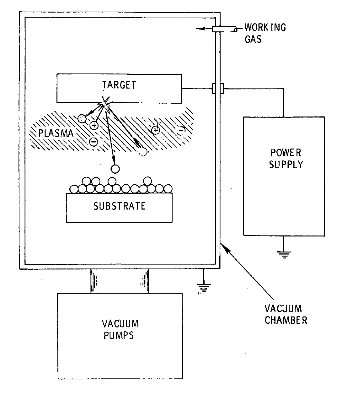
Substrates
The substrate is the foundation on which the thin film components are built. The substrate properties have significant influence on the performance of the device. Alumina is still the most common substrate material due to its surface quality, cost, and high frequency performance.

Conductor/Resistor Films
Thin film resistors are typically used for precision applications. Their values are very accurate and have an excellent temperature coefficient. Inductance and capacitance are generally lower. Thin film resistors are used in medical equipment, audio installations, precision controls and measurement devices. Thick film resistors are used in lower-cost applications where high accuracy and precision are not needed.

Vias
Vias provide electrical and thermal connections between layers of thin film substrates. The vias are filled with with gold, copper or polyimide depending on the application and cost target. Gold and copper provide highly conductive and reliable connections while eliminating epoxy or solder bleed-through. A polyimide via eliminates epoxy or solder bleed-through but at a much lower cost than the pure metal filled via products.

Cross-Overs & Dams
Polyimide is used to create solder dams – structures that stops the flow of solder from one location to another. Polyimide is also used to create a cross-over, or bridge, on the circuit board.

The Process
Thin Film products begin with a concept for a new circuit. The concept is then turned into a design which can then be put into production. UltraSource is here to help transform your design ideas from concept to reality.
