Polyimide Processing

Unlock the Potential of Your Thin Film Design
New fabrication techniques that improve performance, lower assembly costs, or reduce size are always of interest. Enter Polyimide! Polyimide is a polymer material known for its thermal stability, good chemical resistance, excellent mechanical properties, and characteristic orange/yellow color.
The cured film properties of polyimide allow it to be used as dielectric features in thin film applications in order to provide performance or assembly benefits. Polyimide coatings are being used more and more as customized, integrated 3D dielectric coatings on thin film circuits and interconnects. The associated cured film properties are well suited for high performance electronics applications.
Photosensitive polyimide coatings are applied at the substrate level using standard thin film photoresist processes and equipment. In fact, it behaves just like a photoresist. After exposure and developing, thermal curing converts the film into a robust cured polymer. Cured polyimide is well suited for high performance electronics applications. The associated cured film properties are shown in the table.
| Typical Polyimide Properties | |||
|---|---|---|---|
| MECHANICAL | Tensile Strength | MPa | 200 |
| Young’s Modulus | GPa | 3.5 | |
| Water Absorption | % | 1.3 | |
| THERMAL | Glass Transition Temp | °C | 325 |
| CTE | ppm/°C | 35 | |
| Thermal Decomposition Temp (1%) | °C | 410 | |
| ELECTRICAL | Dielectric Constant | 3.3 | |
| Dissipation Factor | .001 | ||
| Dielectric Strength | kV/mm | 250 | |
| Volume Resistivity | Ohms/cm | 2.4×10¹⁶ | |
The cured film properties of Polyimide
POLYIMIDE COMMON USES
There are four common uses of polyimide coatings that thin film circuit designers should be aware of:
SOLDER DAMS – A polyimide solder dam is a strip of material placed strategically across lines or pads to stop the flow of solder from one location to another.
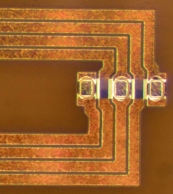
CROSS-OVERS – In Lange Couplers and similar devices where there is a need to replace wirebonds with a robust cross-over, we often use polyimide as a permanent cross-over. Cross-overs supported by polyimide provide a rugged, highly reliable structure.
MECHANICAL PROTECTION LAYER – Polyimide is very useful as a mechanical protection layer. It is used to protect fine pitch or critical circuit areas from assembly damage.
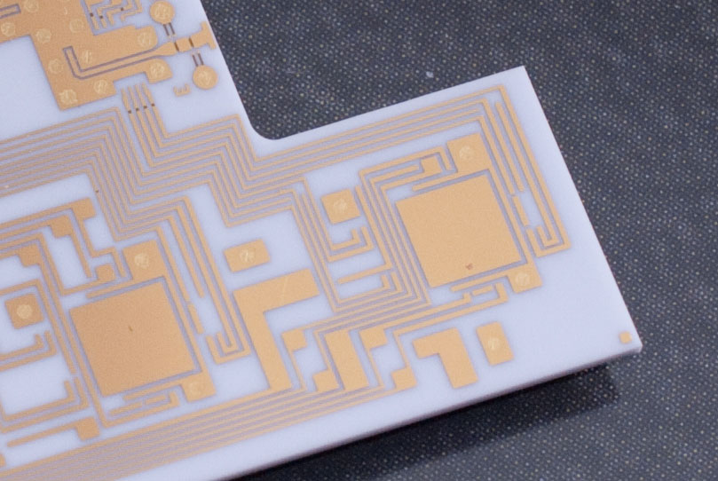
MULTILAYER – Polyimide offers the ability to build up multiple layers of circuitry and dielectric on thin film circuits on ceramic, thus providing the ultimate process for reducing size and increasing signal speed.

Polyimide supported Cross-over in Lange Coupler

Sample of Multilayer Design
Polyimide Advantages
The combination of the superior material properties of polyimide and the dimensional resolving power of thin film technology enables many functional advantages:
- Solder Dams, Cross-Overs, Mechanical Protection Layers, and Multilayer construction are new features becoming mainstream on today’s thin film designs
- High level of 3D vertical integration provides many thin film design improvement possibilities
- The ability to integrate in 3D can increase circuit density, reduce total costs, and provide high frequency performance that cannot be achieved with conventional 2D planar circuit architecture
- The Multilayer technology opens the door for real multifunction chips that combine analog, digital, RF or microwave, and optoelectronic functions


