Photomask Layout & Design

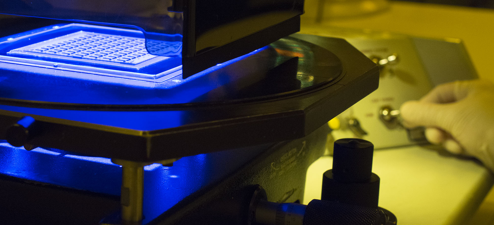
Customer supplied CAD designs are drafted into a step & repeat pattern in order to maximize substrate yield and provide the lowest cost and highest quality thin film devices. Etch factors, alignment features, and photomask polarity are added according to the specific thin film process and/or substrate requirements.


