ENEPIG – The Universal Finish
ENEPIG is the acronym for Electroless Nickel (EN) Electroless Palladium (EP) Immersion Gold (IG). ENEPIG, defined in specification IPC-4556*, has been adopted as a standard plating scheme for applications including soldering, wirebonding and as a contact finish.
*Note: IPC is the Institute for Interconnecting and Packaging Electronic Circuits.
ENEPIG is a surface finish system that is compatible with both gold and aluminum wire bonding, but also provides high-strength soldering. ENEPIG eliminates reliability issues related to reduced solder joint strength with gold (embrittlement).
A common challenge in high density (HD) thin film circuit design and manufacturing is balancing the competing needs of Gold wirebonding and surface mount soldering on the same circuit. Gold wirebonding processes typically require a minimum of 80 microinches of Gold in order to form high-strength, reliable wirebonds. However, most surface mount soldering processes suffer from reduced solder joint strength and reliability at these Gold thicknesses due to Gold/solder dilution which causes embrittlement of the solder joint. Historically, there have only been two thin film metalization solutions for HD applications that require wirebonding and soldering on the same circuit.
Why ENEPIG Is Necessary
For many years, the most common approach in HD applications has been to use the same metal stack across the entire circuit, with the Gold thickness being at least 80 microinches to allow for Gold wirebonding. A typical example of this metalization is shown below. This scheme uses an adhesion layer of WTi (90% Tungsten/10% Titanium) followed by a 20 microinch barrier layer of Nickel (Ni), followed by a Gold layer of 100 microinches. However, these days, this approach is mostly used for building quick turn prototypes or engineering builds due to Gold embrittlement concerns.

Cross-section of typical WTi/Ni/Au metallization
An alternative to using the same metal stack across the entire circuit has been to apply a thick wirebondable Gold layer across the entire circuit, with a solderable metalization applied selectively to specific areas, shown below. This approach alleviates the Gold embrittlement concerns at the solder joints, but adds complexity and cost to the metalization and patterning processes. Photolithography and etching costs are typically double, as the material must go through separate patterning steps. This construction method is often not competitive for cost sensitive solutions.

Cross-section of wirebondable thick Au with selective Ni/Au or Pd/Au solder pads.

| Immersion Gold | 1.2 microinches minimum |
| Electroless Palladium | 2-12 microinches |
| Electroless Nickel | 120-240 microinches |
| Copper | 160-240 microinches |
Thicknesses of the four ENEPIG layers
The elimination of Lead from electronic devices, as mandated by RoHS (Restriction of Hazardous Substance), is changing the playing field for companies that manufacture and supply electronic assemblies globally. Lead-free SAC solder (Sn/Ag/Cu alloys) are the new solders of choice that enable RoHS compliance but these solders suffer from poor joint strength when used with classic Gold or Nickel metalizations.
In the ENEPIG metalization scheme, the Palladium inhibits Nickel diffusion into the Gold layer, promoting long term shelf life (before assembly) benefits. During SAC soldering, the Electroless Palladium provides excellent solderability and can withstand multiple rework cycles. The solder strength of SAC solders to ENEPIG is very high. Both Gold and Aluminum wire bonding can be performed on ENEPIG.
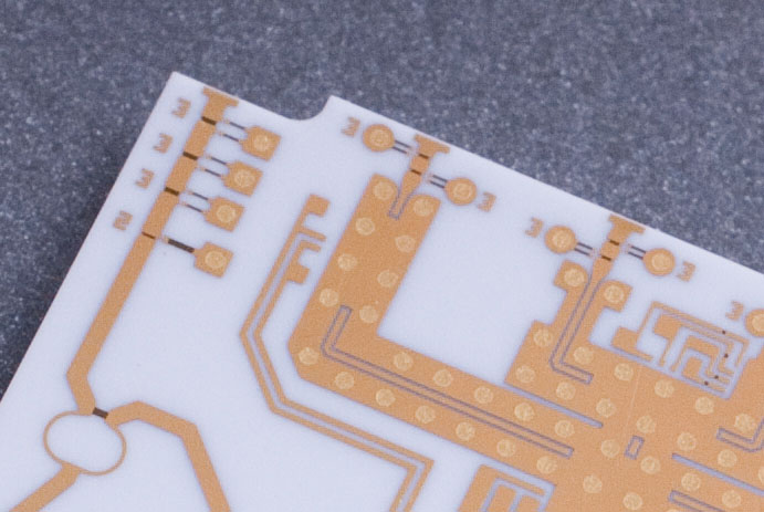
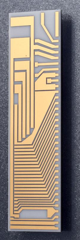
UltraSource has developed a thin film based ENEPIG process that now combines low cost sputtering, traditional thin film photolithography and etching, and plating with ENEPIG. The process is well suited to volume applications. Because the ENEPIG finish is plated and contains very small amounts of precious metal, it is intrinsically less expensive than traditional thin film choices for providing wirebonding and soldering on the same circuit.


